For us, process development means a holistic technology concept that explores feasibilities and thus addresses current requirements. The current project for the development of an efficient joining process for microsystem technology is representative for the research work in the department of process development.
In this project, the CiS Research Institute is working with the Fraunhofer IWS Dresden and the Hahn-Schickard-Gesellschaft Villingen-Schwenningen on the process integration of RMS layers (Reactive Multilayer Systems) as joining material for chip and wafer bonding processes based on novel zirconium systems. This material combination has decisive advantages for further process steps in microsystem technology.
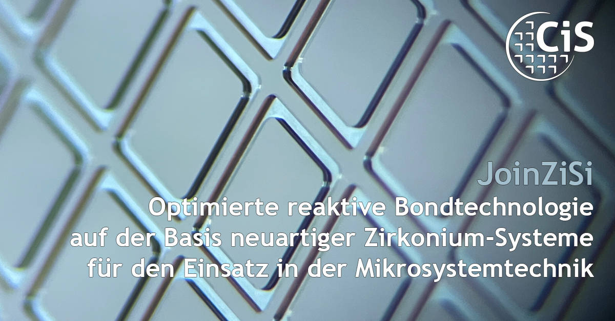
The focus of the work at the CiS Research Institute is on wafer bond technology. In the first step, a structuring process was developed and tested. A lift process (Laser Induced Forward Transfer) was developed for the almost 30 µm thick RMS layer system, which consists of a double resist layer system and has a total thickness of more than 70 µm. An RMS layer is built up from many, nanometer-thin alternating layers.
The process suitability for a base metallization via chemical Ni/Au, the RMS layer deposition and the final lift-off process was successfully demonstrated. For this purpose, an ignition technology was worked out and the wafer bonder was adapted to the process conditions. Ignition triggers a chain reaction. The materials are joined together in fractions of a second. Initial tests demonstrate the feasibility of joining technology via RMS systems at wafer level. The investigations into wafer-level bonding are currently being continued and joining process parameters optimized.
 The research and development work in the project “Optimized reactive bonding technology based on novel zirconium systems for use in microsystems technology” (JoinZiSi) is funded by the German Federal Ministry of Economics and Climate Protection.
IGF project no.: 21347 BG


