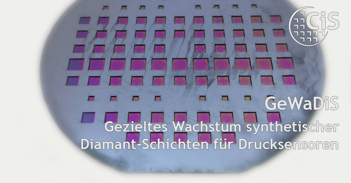
Sensors are often exposed to aggressive environmental conditions. The sensitive surfaces of the sensors are protected by surface passivation. Especially synthetic diamond layers can increase the chemical resistance of the components if they can be manufactured and processed in a cost-effective, CMOS-compatible way. In the GeWaDiS project, diamond layers were applied to relevant local sensor areas of silicon-based sensors in order to avoid post-processing of the layers (structuring). The method was tested on piezoresistive pressure sensors and impedance sensors. With different technological approaches it was proven that:
- a synthetic diamond layer can be successfully implemented as passivation of MEMS devices,
- the passivation quality of the diamond layers is better than that of the reference passivation in the aggressive media examined,
- the application of the diamond seed layer is possible over the entire surface,
- the diamond seed layer can be applied locally and highly selectively via an adapted inkjet process on flat surfaces and also on/in 3D structures,
- this selectively applied seed layer in the inkjet process led to highly selective diamond growth in
- the subsequent synthesis process, which means that structuring of the diamond layer is no longer necessary,
- the implementation of the application of the diamond passivation layer in the low-temperature process in the back-end process is promising, as compatibility aspects and purity can be left out,
- a cost-effective and simplified process for the application and structuring of synthetic diamond coatings could be implemented
In summary, synthetic diamond coatings represent a very good passivation of MEMS devices against chemically aggressive media. Due to the developed process sequence, which allows local growth of the layers and thus eliminates the need for complex structuring, a simple and uncomplicated implementation in the production of silicon sensor elements is possible.


