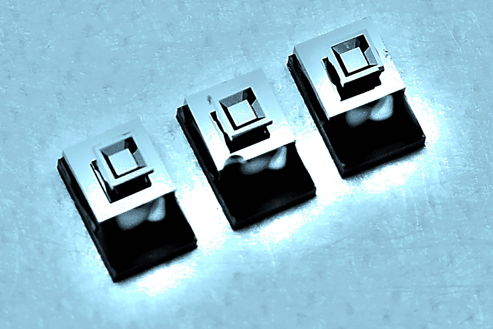
Barometric MEMS pressure sensor for bio- and medical technology – edge length 1 mm
At Sensor+Test 2017, the CiS Forschungsinstitut für Mikrosensorik will present highly stable, media-resistant barometric pressure sensors in MEMS technology. As a research institute, CiS offers industrial customers technological solutions and accompanies the transfer from functional prototype to series production in accordance with ISO9001 certification.
In addition to the goals of miniaturisation and reliability, the development of the MEMS pressure sensors focused on long-term stability and chemical resistance of the surfaces in contact with the media. Without protective coatings in the form of oils or elastomer layers, the sensor elements, which are manufactured in a plasma deep etching process, can be used directly, e.g. in medical applications or in micro-reactors in biotechnology.
The absolute pressure sensors presented here with 1 mm edge length and embedded piezoresistors typically deliver 20 µV/hPa sensitivity with measurement accuracies of up to 1 Pa. Due to the high resolution, they are also suitable, among other things, for indoor navigation or monitoring tasks, such as fall detection of patients.
With the plasma depth etching process, shapes of cavities and chip contours can be realised that are not possible with wet etching processes. Even round cavities and sensor chips are possible for special applications. The functional sensor element is assembled by wafer-level packaging (WLP), using flip-chip interconnects and silicon through-silicon vias (TSVs), among other techniques, for 3D integration. With corresponding quantities, the production costs are quite comparable with conventional technologies.
Based on the manufacturing technology developed, further projects are already being planned. These include the contacting of the WLP sensor modules on ceramic conductor carriers with glass solders, the realisation of multi-chip modules and the development of piezoresistors, coatings and assembly techniques suitable for high temperatures. The vertical integration of the sensor chips on customer-specific ASICs is usually carried out without bond wires by means of corresponding interposers with through-platings in TSV technology.
 Parts of the research and development work presented were funded by the Federal Ministry for Economic Affairs and Energy in the projects WPT (Funding code: MF120009) and RUDIS (Funding code: MF150176).
Glossary
MEMS: Micro-Electro-Mechanical Systems
MOEMS: Micro-Opto-Electro-Mechanical Systems
WLP: Waver-Level-Packaging
TSV: Through Silicon VIA
VIA: Vertical Interconnect Access
Interposer: Rewiring carrier / contacting adapter in chip dimensions


