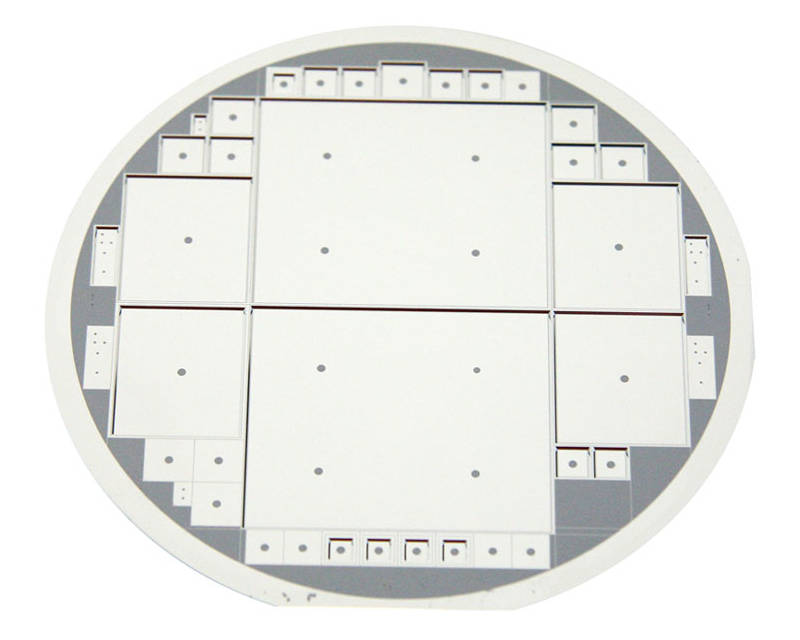
Fig. 1: Back of an etched wafer
The CiS Forschungsinstitut für Mikrosensorik has developed large-area radiation detectors whose sensitive area is thinned down to the thickness of a normal sheet of paper. During processing, it was possible to dispense with the use of additional handling wafers, as is still common practice in industrial production today.
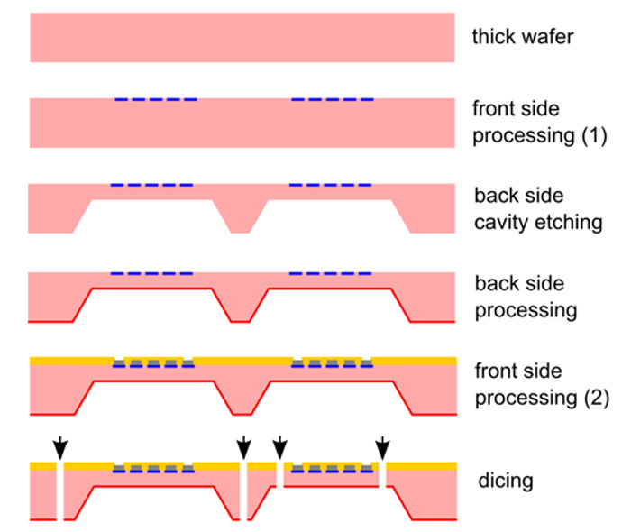
This result was achieved in the research project LAT “Large Area Thinned Radiation Detectors”, in which the technology of wet chemical etching of cavities on large area radiation detectors (Fig. 2) was successfully applied for the first time. In this process, the silicon substrate on the back of the wafer is etched down to the desired target thickness along inclined flanks using KOH solution.
One advantage of this wafer-level technology is the achievable high mechanical stability, which is ensured by the non-thinned frames of the sensor edges and thus simplifies subsequent manufacturing steps, but also helps to reduce assembly costs.
The active sensor areas are located on the thinned membranes with thicknesses between 50 and 150 µm (Fig. 3). This concept favours low operating and depletion voltages, ensures low leakage currents and improved signal-to-noise behaviour of the radiation detectors. Ultimately, this increases the radiation resistance of the sensors and improves the functionality and reliability of the detector.
For future radiation detectors – especially for high-energy physics experiments at the European Nuclear Research Centre CERN – such thin detectors with a relatively large surface area must be produced cost-effectively and in very high quality. The CiS Research Institute has successfully achieved this with a first prototype production of 4×4 cm² pixel sensors (Fig. 1) for use in what is currently the world’s largest particle accelerator, the Large Hadron Collider (LHC).
This provides an alternative manufacturing process for large-area radiation detectors that conserves material resources, reduces additional costs and enables a high sensor yield. Customers also benefit from lower assembly costs at the point of use, e.g. through automation, as well as higher performance and reliability in sensor operation.
By 2017, it is planned to transfer the technology from 4″ to 6″ wafer size to demonstrate decisive advantages in the cost-effective production of thinned large sensor areas.
 The research and development work on LAT is funded by the Federal Ministry for Economic Affairs and Energy (Funding code: MF 140163).
Project presentation at:
Hannover Messe, 25-29 April 2016, Hannover, Hall 4 Stand F34
SENSOR+TEST, 10-12 May 2016, Nuremberg, Hall 5 Stand 5-364
Fig. 2: Schematic process flow
Fig. 3: Measurement of membrane thickness fluctuation


