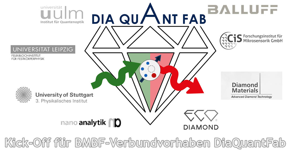
The BMBF joint project DiaQuantFab started on 15.5.2019. Within three years, the project partners will develop commercially viable microsensor systems for high-precision magnetic field measurement and calibration-free current measurement based on NV centres in diamond. To this end, manufacturing technologies will be tested and optimized for industrializability along the value chain. For the first time, the definition of quality standards for the industrial use of the trend-setting quantum material diamond is also being worked on. The project partners are Balluff GmbH (Neuhausen a.d.F.), Diamond Materials GmbH (Freiburg i.Brsg.), EcoDiamond GmbH (Kavelstorf), nano analytik GmbH (Ilmenau), University of Leipzig (Prof. J. Meijer), University of Stuttgart (Prof. J. Wrachtrup), University of Ulm (Prof. F. Jelezko) as well as the CiS Forschungsinstitut für Mikrosensorik (Erfurt), which also coordinates the joint project.
Synthetic diamond as a sensory element
Synthetic diamond can be intentionally contaminated with impurities. What would intuitively be considered disadvantageous opens up a spectrum of fascinating properties and possibilities: Diamond as a particularly stable form of carbon is specifically doped with nitrogen and healed. Nitrogen vacancy centres are formed (NV centres). These are optically active and are therefore also called color centers. With the help of these NV centers, physical effects can be observed at room temperature that can only be described by quantum physical approaches. In addition, the state of the NV centers can be optically stimulated and read out. In recent years, a number of widely acclaimed scientific papers have been produced that are dedicated to potential sensor applications.
One of these applications is the highly precise determination of magnetic fields: Due to the change of the spin state of NV centers by an external magnetic field, their emission behavior also changes as a function of a coupled electromagnetic alternating field. The strength of the external magnetic field can be inferred from the optical luminescence signal read out. Based on the principle of optical excitation and readout of NV centers in external magnetic fields, contactless direct access to the strength of a magnetic field with highest precision and accuracy is achieved. Likewise, electrical quantities directly correlated with magnetism (e.g. electrical current) can be calculated. In the project different applications are developed and evaluated from an industrial point of view: A macroscopic magnetic field sensor for industrial applications as well as a magnetometer for microscopic scanning probe methods are developed by the project partners. These approaches will also be evaluated in another demonstrator, the ammeter for the determination of electrical current. For these applications, the industrial partners have developed recycling approaches.
Standards for the industrial use of synthetic diamonds as “quantum material
The availability of synthetic diamond materials has increased in recent years due to a global increase in manufacturers. Prestigious is the use as gemstone. The largest market volume comprises the abrasives industry, which appreciates the outstanding hardness of the material. The quantum material diamond, on the other hand, addresses optoelectronic applications and is relevant for many different applications in quantum technology (e.g. sensor technology, communication, cryptography). This offers both opportunities and challenges: In order to be able to offer the required material qualities reliably, reproducibly and cost-effectively, efforts must be made to standardize and standardize measured variables and methods. Uniform material specifications for the specific application must be defined in order to exploit further potential cost savings. Therefore, important parameters for the characterization of synthetic diamonds in different manufacturing phases are measured and evaluated in order to make a proposal for a quality standard with recommendations for the measuring methods. Future users will thus receive uniform quality criteria for high market acceptance.
The project
The joint project “DiaQuantFab – Standardizations in the Production and Processing of Quantum Materials Using the Example of NV Color Centers in Diamond to Realize a High-Precision Amperemeter Based on Quantum Effects” was selected for funding by the BMBF in the call “Key Technologies for Quantum Sensors” (May 2017) and is being subsidized with € 1.8 million over three years. Project duration is from 15.5.2019 to 14.5.2022.
The partners
- Balluff GmbH (Neuhausen a.d.F.): Supplier of industrial sensors and sensor technology
- CiS Forschungsinstitut für Mikrosensorik (Erfurt): Si-based Sensor Technology & Research Transfer
- Diamond Materials GmbH (Freiburg i.Brsg.): Manufacturer of high-purity CVD diamond discs
- EcoDiamond GmbH (Kavelstorf): Manufacturer of individual HPHT diamonds
- nano analytik GmbH (Ilmenau): Manufacturer of various scanning probe technologies
- University of Leipzig (Prof. J. Meijer): FG for Solid State Physics, Manipulation of Diamond
- University of Stuttgart (Prof. J. Wrachtrup): 3rd Physical Institute, NV-based Sensor Technology
- University of Ulm (Prof. F. Jelezko): Quantum optics and diamond growth
The CiS Forschungsinstitut is the coordinator of the project.
More information at www.DiaQuantFab.de


