

Successful workshop on assembly and connection technology
At the workshop “Current developments in hybrid and wafer-level assembly” on 12th September 2023 in Erfurt, experts from mechanical and plant engineering, semiconductor foundries, scientists and AVT experts discussed individual processes in packaging and interconnection technology, their technical status and future potential with a focus on silicon-based microsystems. All participants agreed: the workshop offered numerous, exciting contributions as well as opportunities for exchange, networking and idea generation
Silicon Science Award 2023 presented to Lukas Leon Barthelmann
A total of five outstanding works by young researchers were honored yesterday with the Silicon Science Award. The award ceremony took place on 4th September 2023, as part of the opening event of the international 60th Ilmenau Scientific Colloquium “Engineering for a Changing World” in the Audimax of the Ilmenau University of Technology

Current developments in hybrid and wafer-level assembly
The CiS Workshop with focus on packaging and interconnect technology will take place on 12th September 2023 in Erfurt under the motto “Current developments in hybrid and wafer-level assembly”. Look forward to exciting contributions as well as ample opportunity for professional exchange and networking

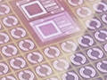
Improvement of the stability of hybrid silicon strain sensors (SiDMeses)
In the SiDMeses research project, the long-term stability of hybrid silicon strain sensors was significantly improved by a targeted and accelerated reduction of the mechanical assembly stress and a precise, extremely parallel and symmetrical structure was generated
Project start Thermopiles with carbon nanotube absorbers
The new project “Thermopiles with carbon nanotube absorbers” investigates the integration of thin coatings of carbon nanotubes on thermopiles with the aim of enabling higher absorption at low cost
Project start KoSenDi: Compact sensor unit for measuring magnetic fields using diamond fluorescence
In the newly started project KoSenDi (Compact Sensor Unit for the Measurement of Magnetic Fields Using Diamond Fluorescence), scientists at the CiS Research Institute are working on the miniaturization of a magnetic field sensor based on sticksoff defects (NV centers) in diamond
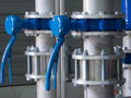
Project start NivLer: Retrofit kit for non-invasive pressure measurement
The new research project NivLer at the CiS Research Institute addresses the development of a retrofit kit for non-invasive pressure measurement in process pipes in order to be able to non-destructively record and digitize various condition variables
Project start DiaTip: Active diamond-based scanning probes for QUANTUM metrology and nanofabrication – development of hybrid assembly methods
The CiS Research Institute is partner of the started joint project “DiaTip”. Together with the partners, the efficient production of diamond tips as well as a suitable assembly process for the joining of two components “active microcantilever” and “diamond tip” shall be developed

Novel material combinations and sensor geometries for resistance thermometers in the hydrogen economy
In the new project Cryo-Resistance both the further development of industrially manufactured resistance thermometers in cooperation with UST Umweltsensortechnik GmbH and several layout variants based on semiconductor technologies of the CiS Research Institute are pursued
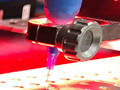
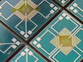
Hybrid integrated optical sensors based on pre-structured adhesive layers
The “Hivos” project follows the industry’s request and aims at higher automation by deposition and patterning of adhesive coatings at wafer level and the associated improved assembly accuracy. Innovative materials and processes are also intended to increase value creation at wafer/benefit level