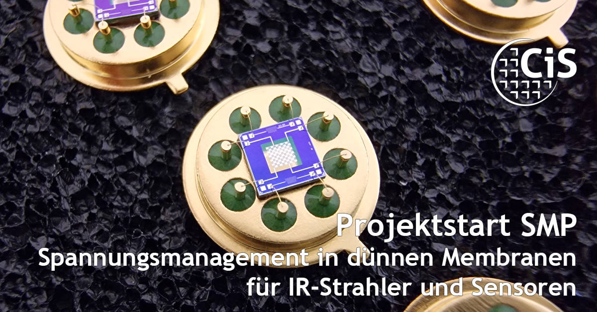
The project “Voltage management in thin membranes for IR emitters and sensors”, which was launched at the beginning of November 2023, is dedicated to the important technology optimization for the production and operation of infrared (IR) sensor chips. Such IR emitters and detectors are used, for example, in gas or contactless temperature measurement systems, such as those used in medical technology and process measurement technology. As a functional element, they contain an active zone that is only a few micrometers thick. During the production and thermal operation of the chips, the different materials involved inevitably lead to thermo-mechanical stresses, which can result in deformations and thus to yield losses in production and limited service life in use. As part of SMP, the underlying thermomechanical mechanisms are being researched in greater depth. Using test structures, a material database of the thin layers in question will be developed depending on their deposition parameters. Simulation models based on this will identify critical stress points and compensate for them with adapted sensor designs or reduce them to a tolerable level. The aim of the optimizations is to increase the yield during production and increase the service life of the components in use.
 The research and development work described is funded by the Federal Ministry of Economic Affairs and Climate Action (BMWK) as part of the “Stress management in thin membranes” (SMP) research project.
Fundin code: 49MF230027


