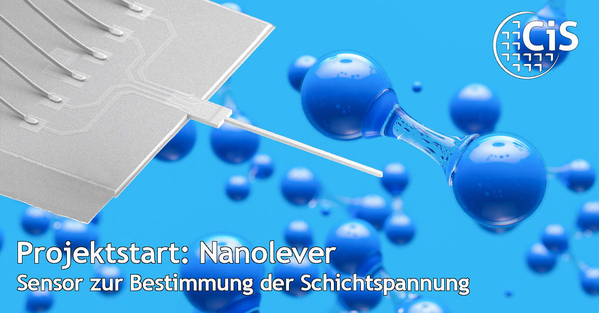
Under the abbreviated name “Nanolever”, a project recently started at the CiS Research Institute with the aim of producing a sensor for determining the layer stress. A number of measurement methods use the layer stress as a physical principle. Here, the deformation of a bending beam due to the stress differences of a bimorph is technically exploited. In the simplest case, this is a bimetallic thermometer.
In the project, the layout of a mechanical bridge, a cantilever beam clamped on both sides, forms the basis for a piezoresistive sensor that determines the film force, which is a measure of the mechanical stresses. High sensitivity to the measurand is achieved with high robustness to the disturbance variables.
Knowledge and optimization of film stresses have fundamental importance for applications in many products, such as optical data storage devices, low-reflection glasses such as eyeglasses, and innovative applications such as concentration measurement, e.g., with immobilized antibodies or sensitive films for hydrogen detection.
A silicon-based MEMS sensor has many advantages for fabrication and application due to the advantages of semiconductor physics, ease of interfacing/integration of electronics for evaluation and data transmission, the possibility of wafer-level fabrication, the associated economies of scale of higher wafer formats, and low-cost fabrication.
For biochemical and medical diagnostics, properties critical to success include high sensitivity, low cross-sensitivity to other substances, and relative insensitivity to fluid motion, which will be investigated in this project.
 The research and development work described is being funded by the German Federal Ministry of Economic Affairs and Climate Action (BMWK) in the research project “Sensor for Determining Layer Stress” (Nanolever).
Funding code: 49VF220011


