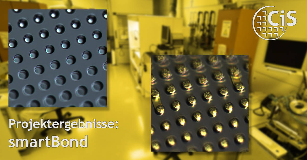
By means of thermocompression bonding with chemical-galvanic deposited pillar structures and their highly accurate positioning by so-called self-alignment, the assembly as well as frictional and electrically conductive joining of photodiodes to hybrid detector modules was optimized. To this end, new assembly technology and the stacking of sensor chips were investigated and tested.
The research team focused on lower process temperatures and higher or more easily achievable positioning precision. Such techniques are required in particular for sensors (or detectors) with a large number and simultaneously small size of the electrical connections or also for sensors with extreme requirements for readout rates and/or energy resolution of the sensor signals. These are in particular detectors with spatial resolution by granular design of the active areas – i.e. with “pixel arrays”. In the field of high-energy radiation (X-rays, gamma, electrons, ions, and other high-energy particles), such detectors are typically stacked on top of application-specific integrated circuits (ASICs), which also consist of an array of signal processing pixels. Lower temperatures and more readily achievable positioning accuracy – as pursued in Project smartBond – increase the applicability of such technologies to sensitive devices and reduce assembly costs.
Results of the work of the project partners CiS Forschungsinstitut and Ilmenau University of Technology were presented in the Jahrbuch Oberflächentechnik Volume 771.
1: Oberflächentechnik Volume 77 (2021): David Glück, Mathias Fritz, Indira Käpplinger, Andreas Bund, “Nickel-Ti3SiC2-Dispersionsbeschichtungen”, Eugen G. Leuze Verlag KG, Bad Saulgau, ISBN 978-3-87480-369-4, pp. 117-125
 The research and development work in the project “Development of a high-precision, form-fit-assisted flip-chip thermo-compression process” (smartBond) was funded by the German Federal Ministry of Economic Affairs and Climate Action.
FKZ: 49MF190065


