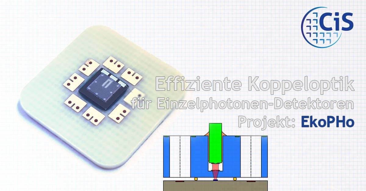
Buzzwords like quantum communication and quantum computers are on everyone’s lips. But what kind of components are actually needed and how can they be produced cost-effectively on an industrial scale? These questions are also being addressed by the CiS Forschungsinstitut für Mikrosensorik GmbH in the newly launched research project EkoPHo, funded by the BMWi.
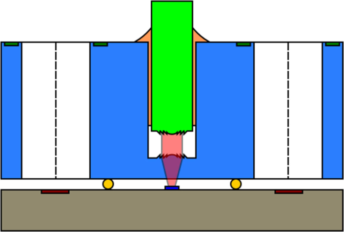
The basis is a package for a superconducting single photon detector, where the electrical and optical coupling is carried out at room temperature and is maintained after cooling down to 4 K. This eliminates any adjustment effort for the user. The package has also been adapted for operation in a closed-cycle cryostat. Based on this, the EKoPho project will further improve the light coupling into the superconducting detector. For this purpose, a coupling optic is written into the chip stack of silicon carrier wafer and superconducting chip in the pit floor of the carrier wafer and the fibre by means of focused-ion-beam (FIB) (Fig. 1). The optics are used on the one hand to focus the light onto the detector and on the other hand to compensate for possible inaccuracies of the flip-chip process. A marker structure on the chips enables the evaluation of the positioning. The micro-optics written after the flip-chip process can thus be used for individual fine adjustment of the chip stack.


