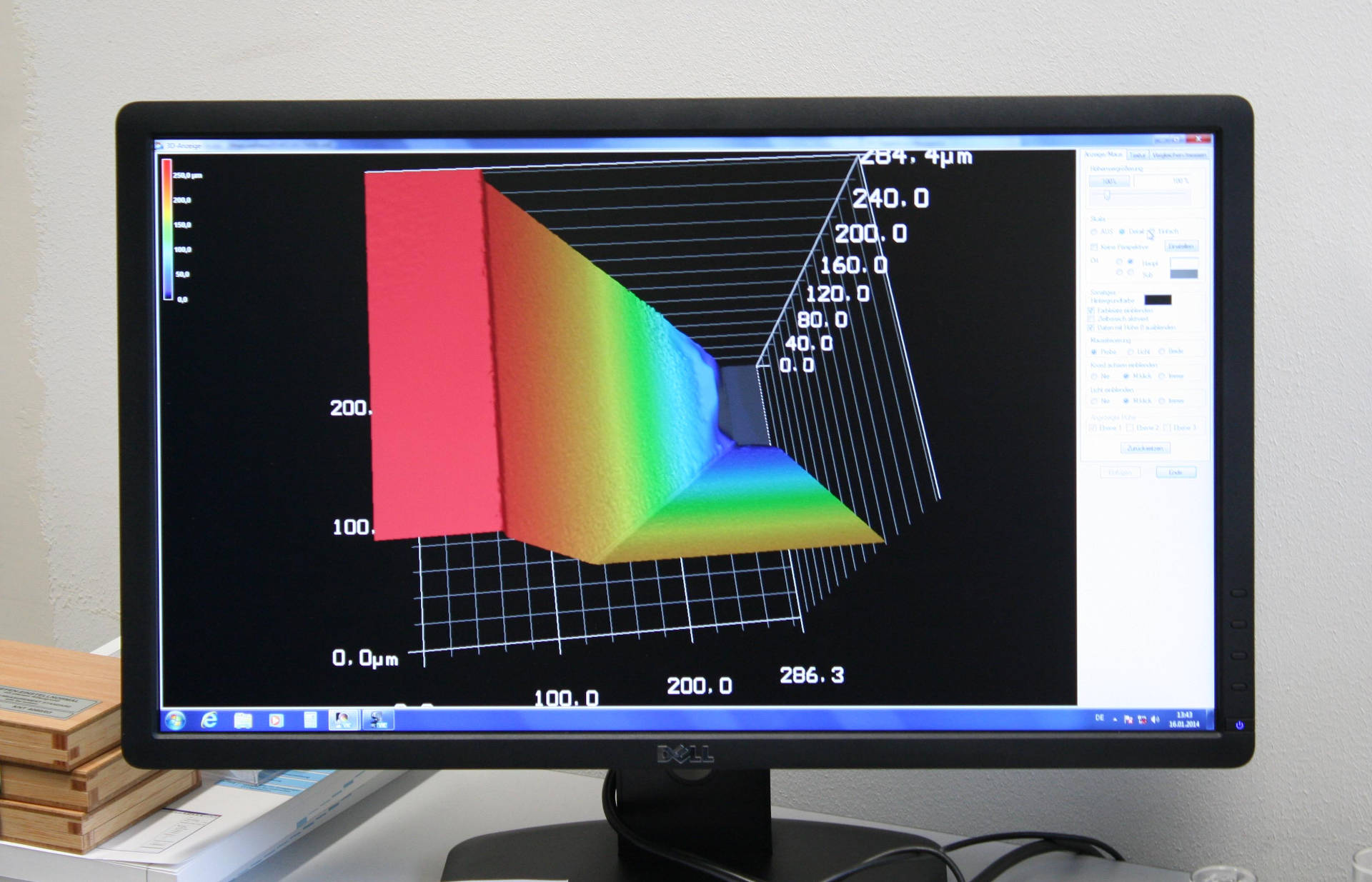
3D surface measurement system
The development of high-performance sensors for harsh-environment environments, coupled with the greatest possible energy savings, is a growing focus in sensor manufacturing.
At the same time, the sensor technology itself is becoming increasingly complex. Cross-sensitivities must be taken into account and eliminated. The intrinsic function control of the sensors to avoid malfunctions is becoming increasingly important. The potential user expects a high degree of reliability, quality and serviceability. Manufacturing technology as well as sensors are tested and characterized with high metrological effort in order to be able to prove the desired properties with long-term stability. Different measurement methods are required for this purpose.
The new semiconductor complex measuring station represents a milestone for the characterization of technologies and sensors. It consists of:
| 1. Waferpober | 8″-Chuck, temperature range: -60 °C … +300 °C |
| 2. Measurement electronics | 48 pin switching matrix, SMUs and CV meters for DC measurements in the fA and fF range or in the DC voltage range µV to 1100 V |
| 3. SIREX measuring station | Measurement of mechanical stresses on or in micromechanical, single-crystalline components (including Si wafers up to 8″). |
| 4. Confocal microscope | Confocal and scanning 3D light microscope with resolution in the range of 20 nm laterally and 2 nm vertically |
Thus, the measuring temperature range of the HKM (-60 °C…+ 300 °C) covers a very wide range of the environmental conditions to be guaranteed for the sensors. Measuring in this range has many advantages. On the one hand, it is useful for controlling systems that previously could not be optimally supplied and controlled due to a lack of suitable sensors. On the other hand, the application systems no longer have to be adapted to the control electronics to such an extent. In addition, cooling power can be saved.
The SIREX measurement method (Scanning Infrared Reflection Examination) visualizes highly precise mechanical stresses in semiconductors, MEMS and 3D IC. This sensitive microscopic method uses a scanning laser beam in reflection mode and evaluates the depolarization. The basis is the optical phenomenon of photoelasticity. The property of many optically isotropic materials to become birefringent under mechanical stress is exploited.
High-resolution images are coupled with a comprehensive characterization of the contact areas and interfaces. The interplay and mutual influence of novel materials among each other and their feedback on the semiconductor materials are also revealed.
In particular for pressure sensor technology, the data obtained will be able to provide new solution approaches for design and technology development. The outstanding feature is the spatially and temporally accurate information on electrically relevant semiconductor phenomena in conjunction with the mechanical characterization of different materials, including their heterogeneous contact interfaces. The semiconductor complex measuring station fulfills these requirements.
Project presentations at:
Hannover Messe, April 25-29, 2016, Hannover, Hall 4 Booth F34
SENSOR+TEST, May 10-12, 2016, Nuremberg, Hall 5 Booth 5-364


