Fiber chip coupling
with 3D diode
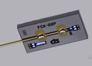
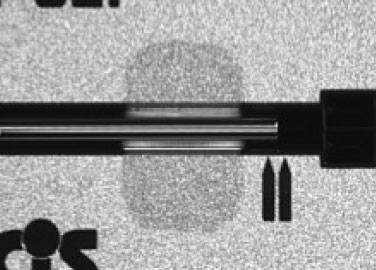
Mounted fiber in silicon cavity (Solderjet Bumping)
The 3D structuring of silicon is becoming increasingly important for optical and opto-electronic applications in microsystems technology. For the reliable and low-loss coupling of optical fibers to photodiodes, the CiS Research Institute developed new microstructuring technologies for the fabrication of cavities with flank angles of 45° and 90° and high optical absorption of the sensitive coupling surface.
In this process, the perpendicular channel in the bulk silicon is used for optimal assembly of the fiber, which is precisely mounted in the silicon substrate using solder jet bumping. The 45° cavities contain photolithographically generated doping regions and contact tracks, so that a pn junction with high spectral sensitivity and bandwidth can be provided for sensing applications. The spectral selectivity of the integrated photodiodes can be customized by bandpass or edge filters.
The new microtechnical concept has been successfully tested in the fabrication of compact 3D photodiodes with PigTail and monomode fibers with 5 μm core diameter. In addition to excellent stability over time and temperature, the following technical parameters were achieved:
RiseTime <1 ns, Spectral response 350-1100 nm.
The optoelectronic module can be operated in high-speed or pulse mode.
For an efficient, cost-effective and industry-suitable production of the microcomponents, batch-capable processes, semi-automated assembly technologies (packaging and interconnection) and certified test and inspection methods are used at the application center microoptical systems of the CiS research institute.
Visit us at the SENSOR+TEST 2012 trade show in hall 12, booth 226 and learn more about our broad range of services in sensor and optics, microstructure and assembly technologies.


