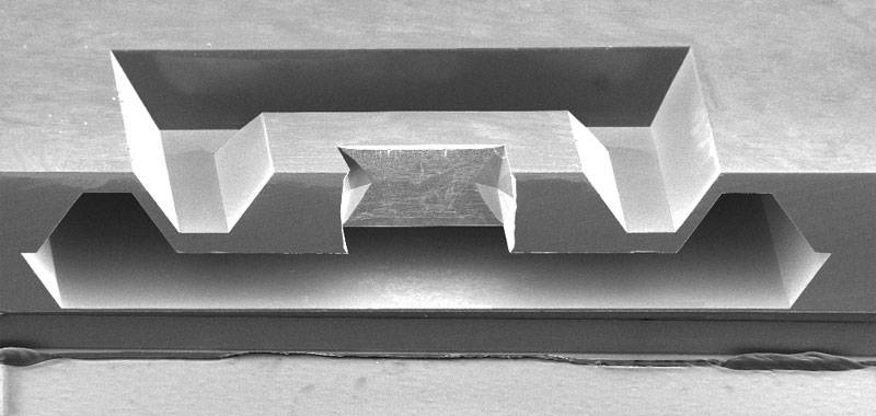
Sensor element joined by low-temperature direct silicon bonding
Low-temperature silicon direct bonding has gained significantly in importance in recent years. In addition to the possibilities of vertical integration, it opens up new process technology opportunities through the application of wafer-level packaging as a post-process in sensor manufacturing.
Plasma activations allow the fabrication of highly stable, multilayer microsystems due to the low process temperatures that can be achieved.
Until now, the production of these systems was subject to significant limitations, since the necessary strength could only be achieved by means of high process temperatures. At temperatures of 700°C and more, sensitive polymers and metallization systems could therefore only be applied and patterned after the bonding process.
The CiS Research Institute has succeeded in lowering the annealing temperature to 325°C by means of a plasma-assisted activation process, thereby achieving a strength for the joining surface that is close to that of the base material. Even at an annealing temperature of 120°C, the activation process still achieves strengths that are sufficient for many applications. This low-temperature process is particularly advantageous when joining partners contain structures made of polymers such as polyimide, hydrogel or SU8.
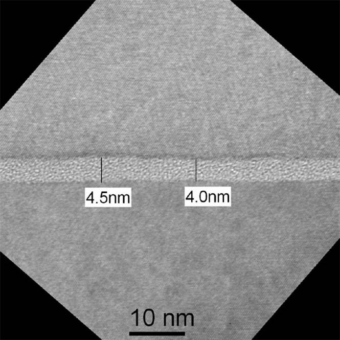
Further advantages are the shorter process times compared to single activation and anodic bonding with borosilicate glass as well as the exact material matching. The results were assessed and evaluated using mechanical fracture tests and physical analysis technologies such as TEM (transmission electron microscopy) imaging, photoelastic stress measurements, IR (infrared) transmission imaging, and ultrasonic microscopy, among others.
Furthermore, a spectrum of analytical technologies is available to improve the performance, stability, and package shape of MEMS chips with a focus on surface homogeneity and low defect levels in preparation for direct silicon bonding.
Please visit us at the SENSOR+TEST 2012,
MNT-Thuringia joint booth hall 12, booth 226.
TEM images of bond interfaces (provided by Fraunhofer Institute for Materials Mechatronics on behalf of CIS)


