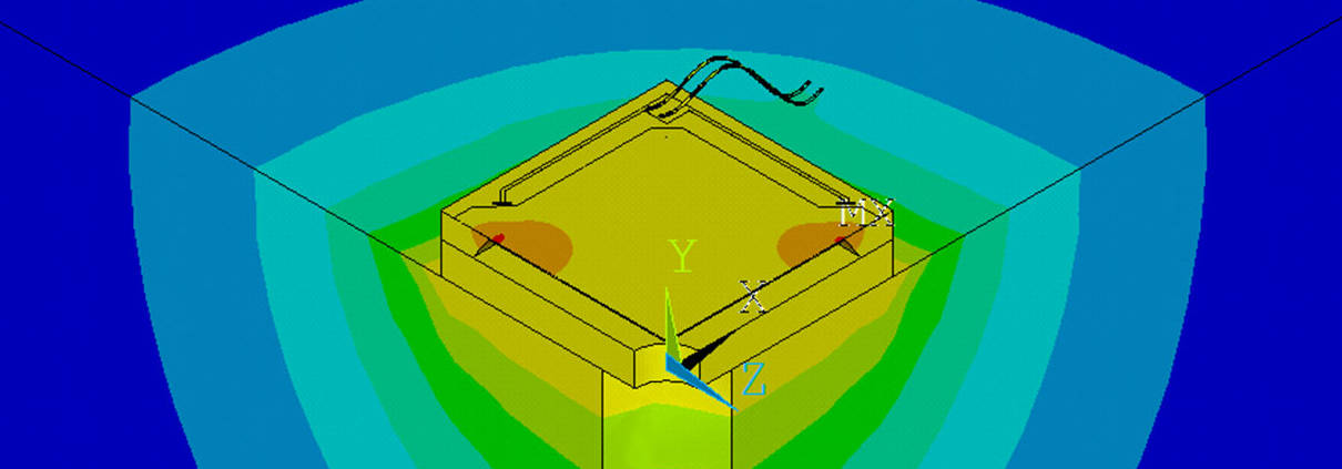
Every development of microsensors begins with the modeling of the physical and technological relationships and the design processes based on them.
In the context of prototype developments, the Simulation and Design department is responsible for the geometric design of the sensors and the technological sequence as well as individual parameters of the manufacturing steps.
The focus of the work is on the design and construction of new or optimized customer-specific microsensors. This design process is characterized by the simulation of semiconductor physical, electrical, optical, mechanical and thermal sensor properties. The design aim is to create the sensor layout with defined design rules and a specific set of test structures for technology characterization and functional verification. Multidomain sensor models with coupling of semiconductor physical, electrical, optical, mechanical and thermal effects can be developed upon customer request, for which extraction of model parameters is possible if high quality sensor measurements are available. The quality of models always depends decisively on the quality of the model parameters. Therefore, a major focus of the work in the Simulation and Design department is on improving the knowledge of the properties of the materials used in wafer fabrication.
Powerful hardware and software tools as well as the coupling to a measurement database are available for all design processes.


