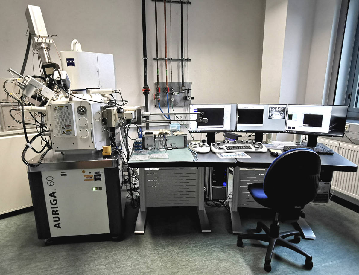
Auriga 60 Crossbeam der Firma Carl-Zeiss
Principle
In a scanning electron microscope (SEM), the surface of a specimen is scanned line by line using a finely focused electron beam guided through electromagnetic lenses and apertures. At the point of impact of the differently accelerated electron beam, various interactions occur on and in the sample surface. Among other things, secondary electrons (SE), backscattered electrons (BSE) and X-rays are produced. All these signals can be registered by detectors present in the SEM. By means of the SE and RE signals, the surface of the samples can be imaged. A high-resolution imaging of the surface is possible especially with the SE. Since the RE yield is element-dependent and increases with increasing atomic number, element differences on the sample surface can be imaged with this signal. The resulting X-ray radiation is not only the non-specific bremsstrahlung, but also the characteristic X-ray radiation, which provides specific energy lines for each element. Thus, the elemental composition can be analyzed at the sample surface. These investigations can be performed even on particles in the µm range.
By means of the ion beam (FIB – Focused Ion Beam), layers on the sample can be ablated selectively and with µm precision. This enables a visualization of the layer structure in these areas.
Technical specification
SEM (Scanning electron microscopy)
- Zoom: 12 – 1,000,000x
- High voltage: 0.1 V – 30 kV
- Resolution: 1.0 nm at 15 kV
- 1.9 nm at 1 kV
- Detectors: SE, Inlens, BSE, Bruker-EDX
- Sample chamber: 520 mm diameter, 300 mm height
- 8″ lock chamber
FIB (Focused Ion Beam) – Canion-Column
- Ion source: Gallium liquid metal source
- High voltage: 1 KV – 30 kV
- Resolution: < 7 nm at 30 kV
EDX (Energy dispersive X-ray spectroscopy)
- Bruker, 30 mm² Si drift detector, 127 eV energy resolution
The Auriga 60 Crossbeam from Carl-Zeiss at the CiS Research Institute


